ER933 Post Dicing Wafer 2D Inspection System
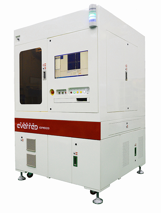
The ER933 is designed to support the semiconductor industry to the high production volume environment and 2D inspection solution for post dicing.
The ER933 is designed to support the semiconductor industry to the high production volume environment and 2D inspection solution for post dicing.

Tel:+886-3-553-5736 Fax:+886-3-553-5739 E-mail: sales@ertek.com.tw Address:No. 765, Zhonghua Rd., Zhubei City, Hsinchu County 302, Taiwan
Tel:+86-510-86131121 Address:No. 201, Jin Shan Road, Jiangyin City, Jiangsu Province, China 214437 (Innovative Industrial Park IT Port, Building D, 1F)